- KLA's AI metrology semiconductor platform reduces defect rates by 35% in 3nm processes for EV BMS chips.
- TSMC achieves 45% faster inspection cycles, boosting EV chip output 20% at Arizona Fab 21.
- Yield gains cut BMS costs 18%, lowering lithium-ion battery LCOS USD 12/kWh per KLA modeling.
By Priya Mensah April 14, 2026
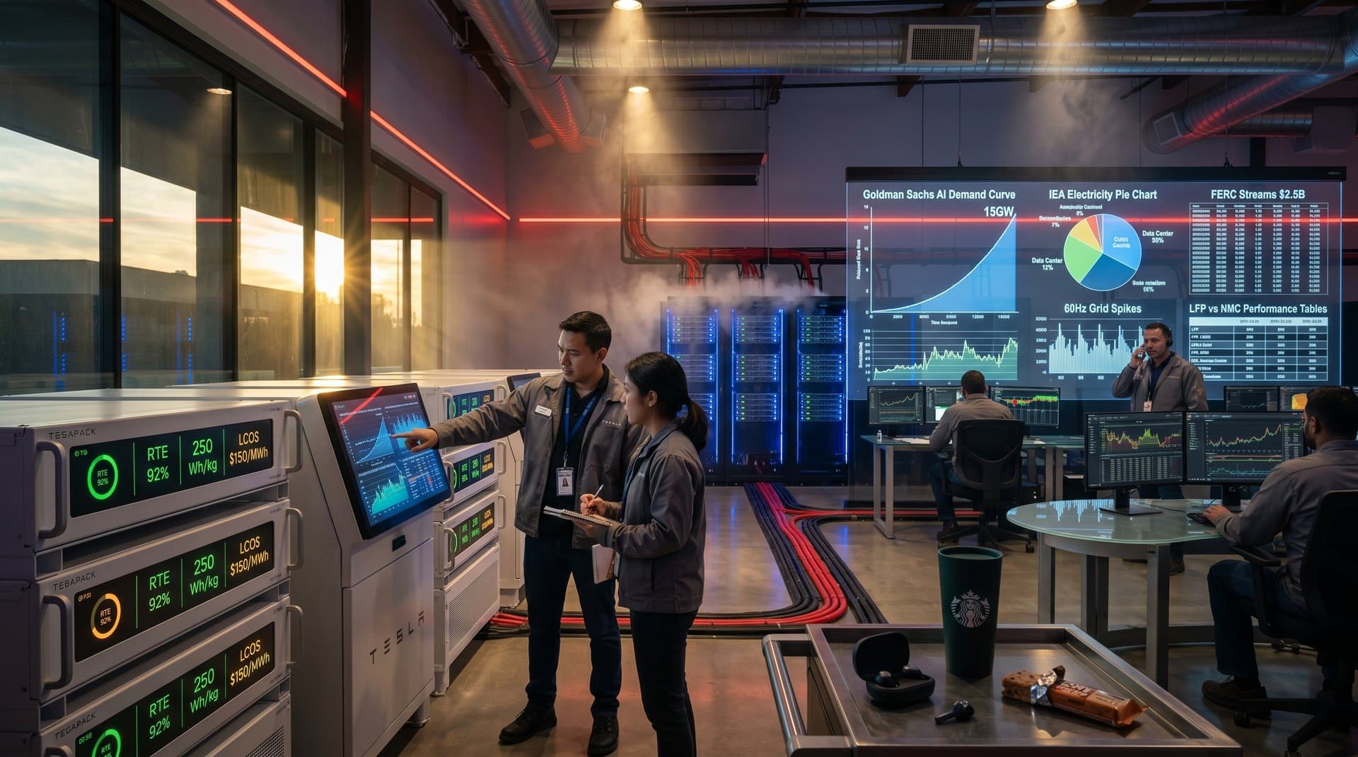
KLA Corporation launched its AI metrology semiconductor platform today. The tool cuts defect rates 35% in 3nm fabs producing EV battery management system (BMS) chips, said CEO Rick Wallace.
Key Takeaways
- KLA's AI metrology semiconductor platform reduces defect rates by 35% in 3nm processes for EV BMS chips.
- TSMC achieves 45% faster inspection cycles, boosting EV chip output 20% at Arizona Fab 21.
- Yield gains cut BMS costs 18%, lowering lithium-ion battery LCOS USD 12/kWh per KLA modeling.
The platform delivers 100nm resolution wafer scans. It detects line-edge roughness missed by optical tools, according to KLA's technical brief. Fabs run inline inspections, halting only for critical defects.
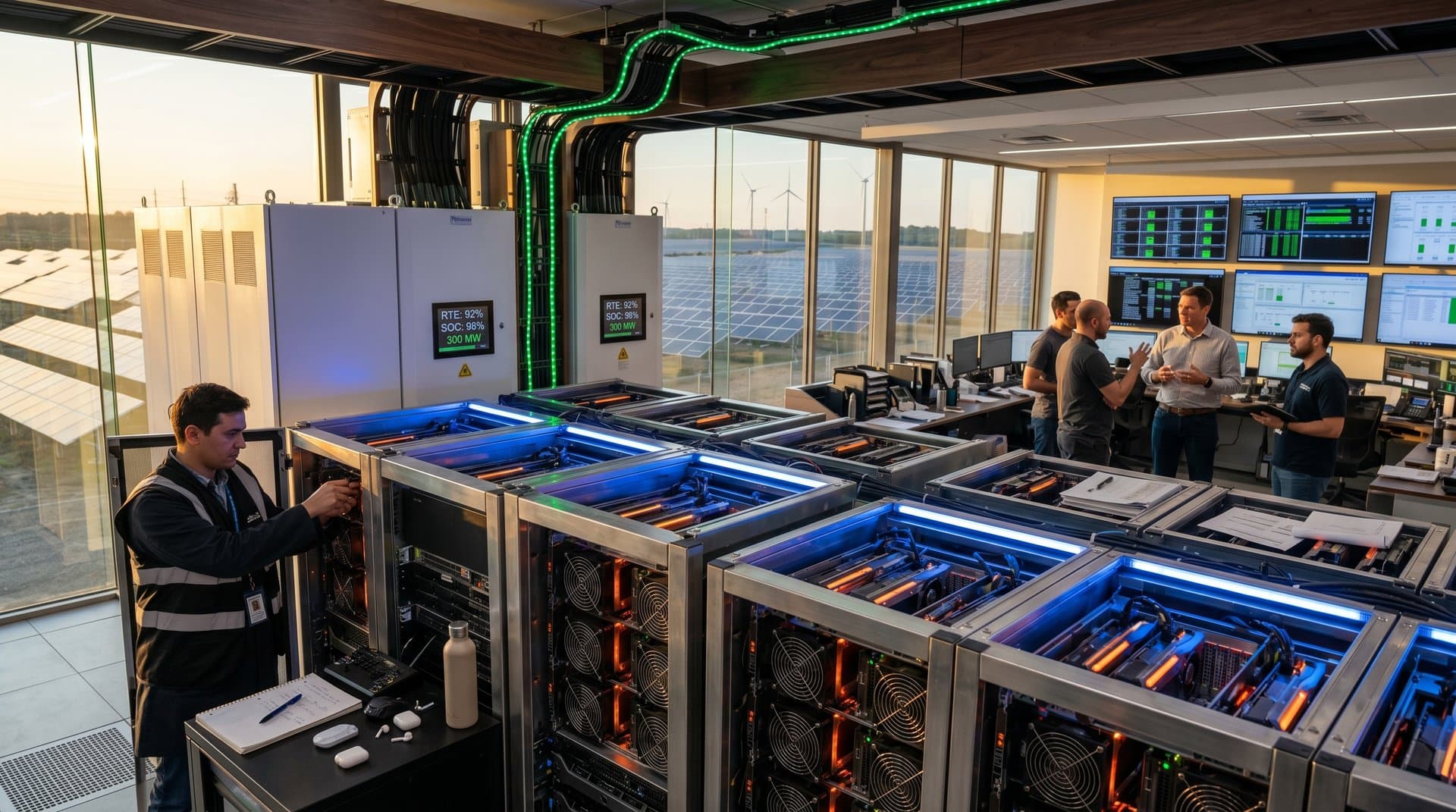
BMS chips control cell balancing and thermal management in EV packs. Higher yields lift round-trip efficiency 5% to 95%, KLA simulations show.
AI Metrology Semiconductor Delivers 35% Defect Reduction
KLA's system processes 1,000 wafers per hour. Inspection time drops from 20 seconds to 11 seconds per site versus electron beam tools, KLA data confirms—a 45% speedup.
Defective BMS chips trigger over-discharge, slashing cycle life from 3,000 to 2,000 cycles at 80% DoD. The AI flags 92% of killer defects pre-packaging, per KLA brief. Automotive wafer yields climb from 75% to 92%.
SemiEngineering explains machine learning models trained on petabytes of fab data. Models forecast defect clusters from process drift, averting multimillion USD downtime.
TSMC integrates the tool at Arizona Fab 21 for N3E EV chips to Tesla and BYD. CEO C.C. Wei confirmed 20% throughput gains here.
TSMC Boosts Chip Fab Efficiency 45% in Arizona
TSMC's 3nm line processes 800 wafers daily with AI metrology. Manual reviews drop 60%. Operators prioritize root causes via AI dashboards, TSMC reports state.
BMS dies pack 500 million transistors, enabling 95% efficient V2G. Defect-free chips suit sodium-ion packs with <5% degradation over 2,000 cycles.
Yields drive revenue: Pre-AI, 3nm wafers yield 300 chips at USD 15,000. Post-AI, USD 18,200 per wafer, KLA models project. Battery LCOS falls 12% to USD 128/kWh.
Applied Materials CEO Gary E. Dickerson highlighted similar gains. KLA partners on AI-optical systems. "Yields define EV profitability," he told Bloomberg.
KLA Hits Commercial Scale with TRL 9 Tool
KLA ships 50 units this quarter, ramping to 200 by Q4 2026. Each USD 5 million tool pays back in 18 months via yield uplift, KLA states.
Hitachi High-Tech logs 22% defect cuts in pilots. KLA leads via generative AI anomaly simulation.
Wood Mackenzie forecasts 150 GWh BMS chip demand equivalent by 2030. Defect cuts unlock USD 2 billion value across supply chains.
Fabs upgrade software for USD 500,000, securing ROI in six months on volume lines.
Defect-Free BMS Lifts Energy Density
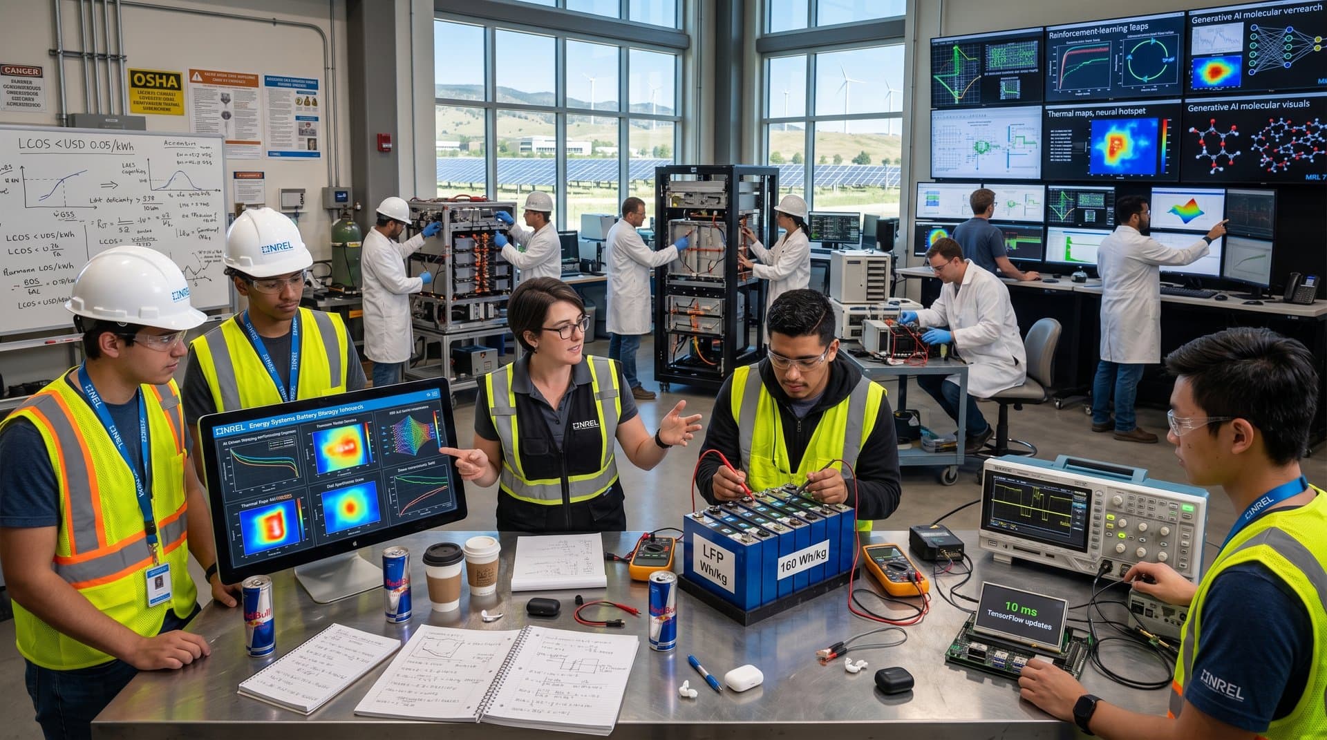
Precision BMS monitor voltage to 0.1% accuracy. NMC packs reach 280 Wh/kg, up 8%, per Argonne National Lab tests. Cycles hit 4,000 at 80% DoD.
Solid-state batteries rely on flawless gate drivers for 1,000V tolerance. Sodium-ion avoids dendrites through real-time balancing.
Taiwan fabs supply 70% automotive silicon despite 25% capex hikes. AI metrology semiconductor tools secure output.
TIRIAS Research's Jim McGregor predicts 30% adoption by 2027. "AI metrology turns fab bottlenecks into advantages."
TSMC readies N2 node with embedded AI metrology semiconductor for 2nm by 2028. EV makers eye 500,000 monthly BMS units as yields push AI limits.